Battery pack

Design, manufacturing and optimization of the UP Karting battery pack.

Battery Pack

Pack topology and BMS selection

For the kart, we decided to use a 48 V nominal battery setup. This was mostly a compromise between keeping the voltage relatively low and safe, not needing too many cells, and still being able to supply the current needed by the motor. Since the motor is rated at 5 kW, the maximum current draw is roughly 100 A, so a 15S configuration made sense.

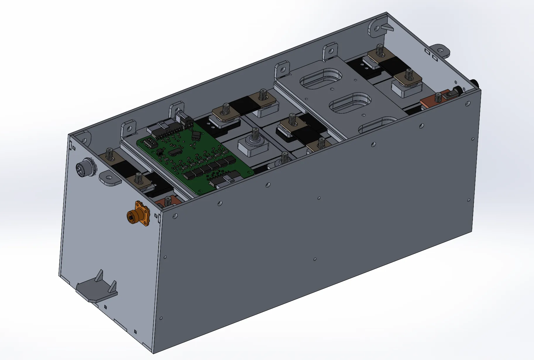
At first, a pack made from cylindrical cells was an option, but in practice it would have made the build more complicated. The main issue was that we did not have proper spot-welding equipment, so assembling a reliable cylindrical-cell pack would have been harder. Because of this, we chose to use high-capacity prismatic cells instead. These are much easier to work with mechanically, since the busbars can be bolted directly onto the cell terminals.

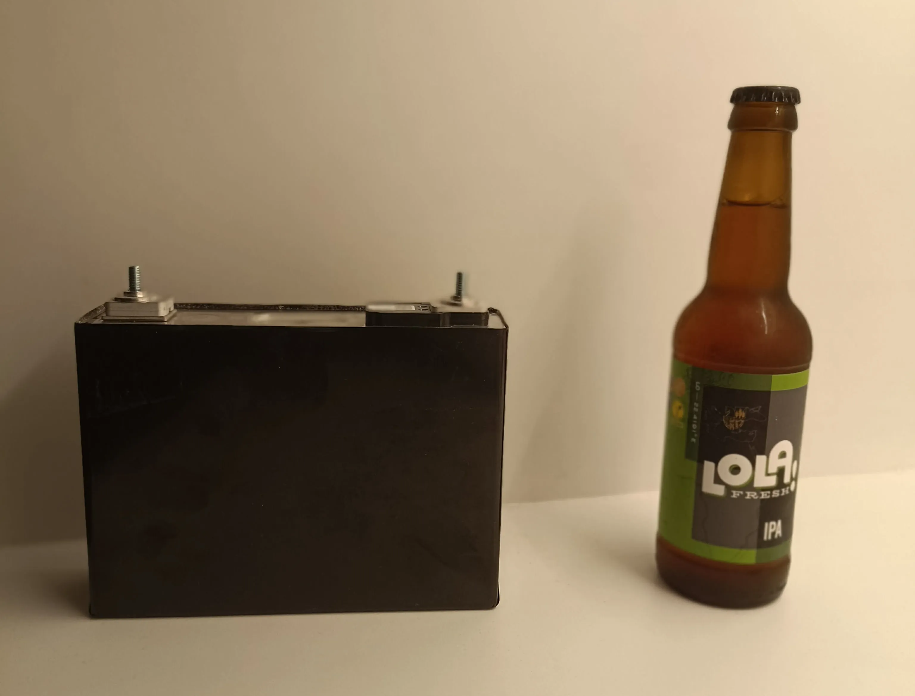
The final battery pack is a 15S1P configuration using Samsung SDI 94 Ah prismatic cells. These cells were a good fit for the project for a few reasons. They have already been used in the BMW i3 battery pack, so they are not an unknown or untested option. They also have a very high maximum current rating of 400 A, which gives us a lot of margin compared to what the motor should normally draw. Their 94 Ah capacity is also more than enough for our application.

Another reason we liked these cells is that they are easier to package than pouch cells. They do not need the same level of compression and careful mechanical support, which makes the battery enclosure simpler. Also, since they are made by Samsung SDI, we had more confidence in their quality compared with many cheaper battery options.

The downside is mainly weight and size. Each cell weighs about 2 kg, so the cells alone add around 30 kg to the kart. They are also quite large, so the complete battery pack takes up more space than a custom cylindrical-cell pack would.

Samsung SDI prismatic cell with a beer can for scale
Samsung SDI, beer for reference

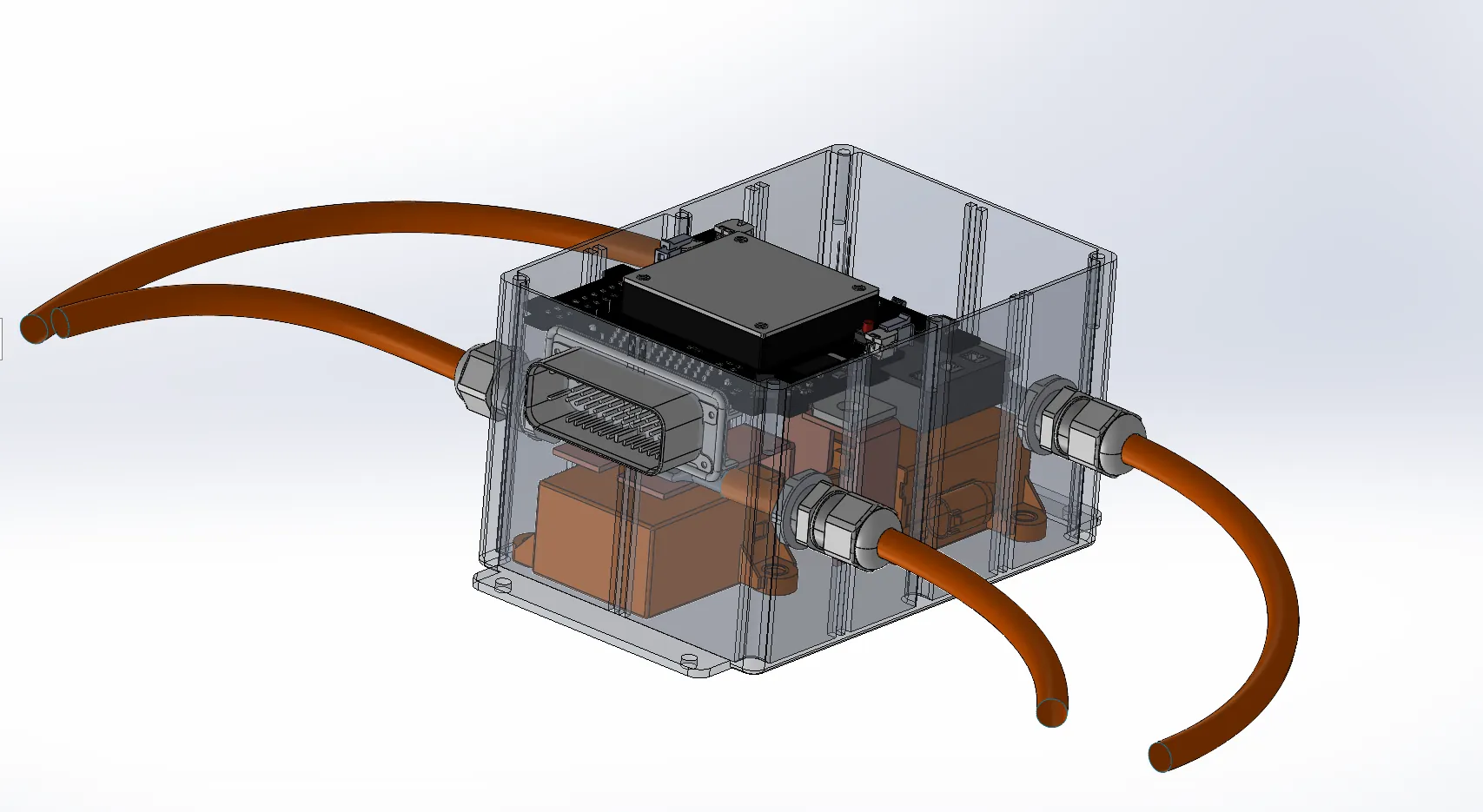
To make the pack fit better on the chassis and keep the weight distribution reasonable, we split it into two parts, one on each side of the kart. One side holds 6 cells and the other side holds 9 cells.

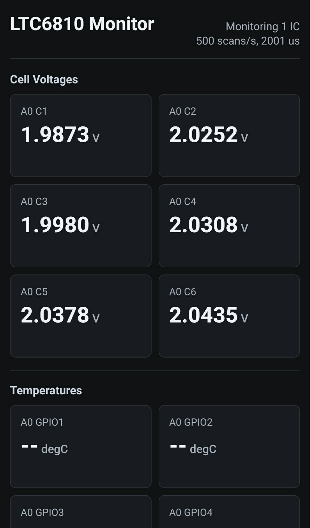
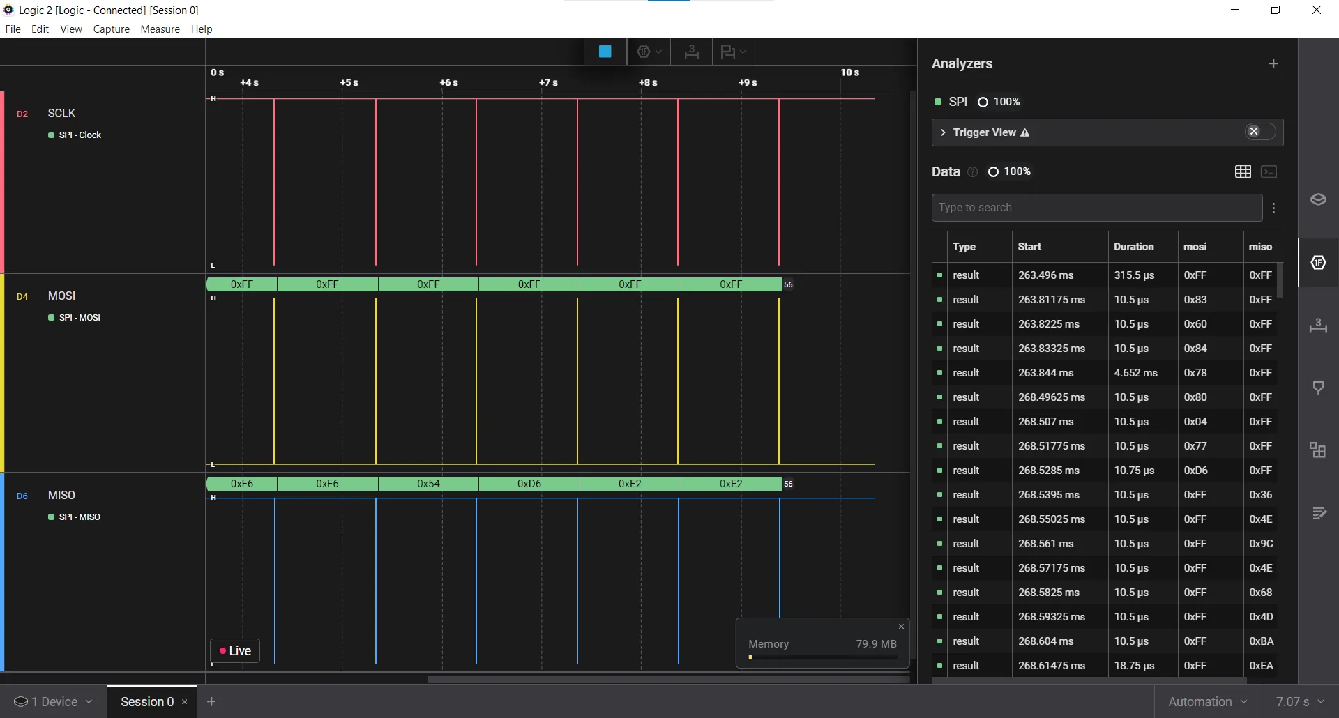
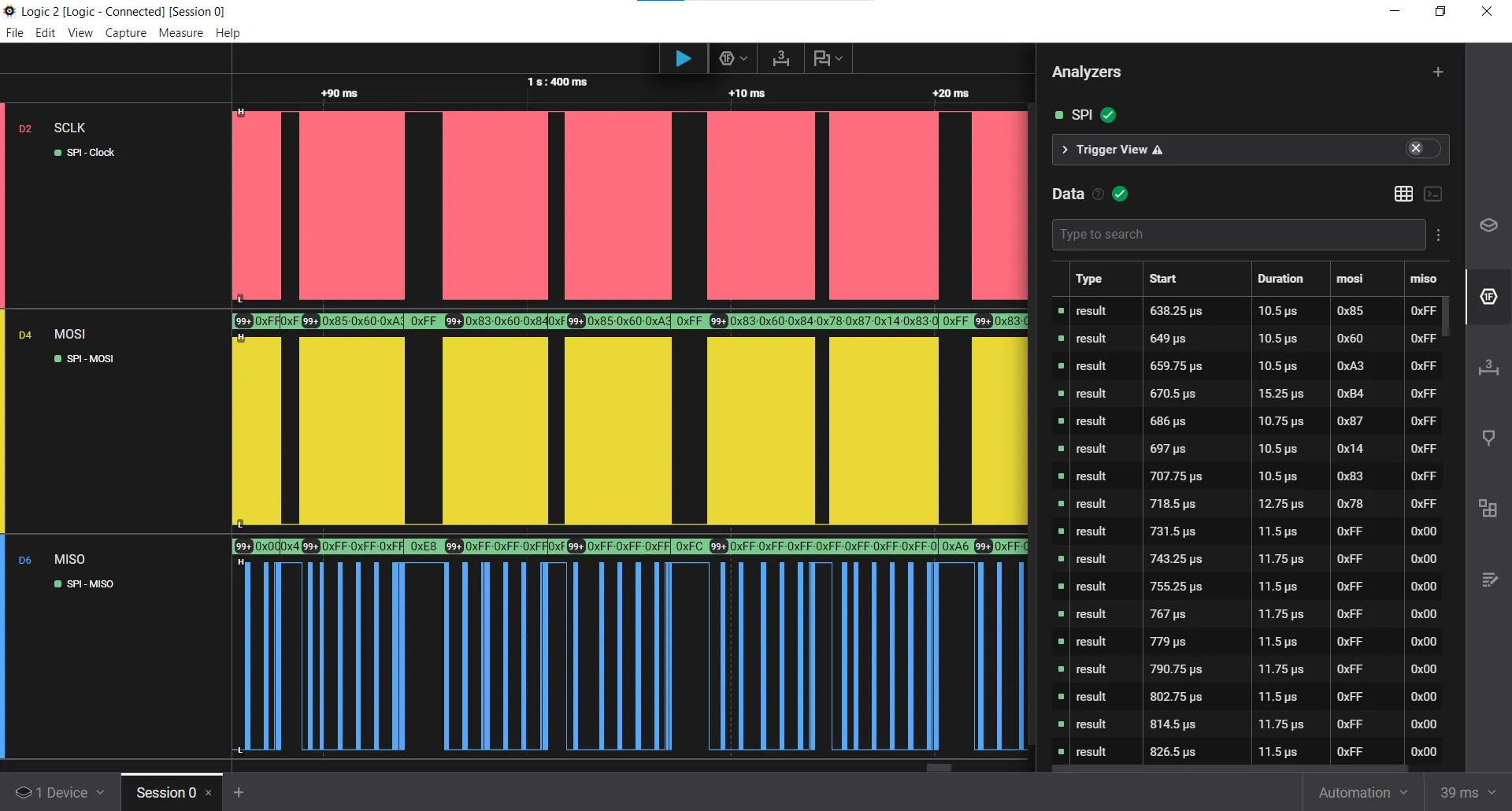
For monitoring the battery voltages and temperatures, we chose the Analog Devices LTC6810 six-cell battery monitor. One useful feature of this IC is that it can operate with a low minimum cell stack voltage, so we can connect only 3 cells to it instead of needing to use all 6 channels. It also uses isoSPI communication, which gives better isolation and noise immunity. This is important in a vehicle, because the electrical environment can be quite noisy and the system is not referenced to a fixed ground in the same way as a normal bench setup.

So in the end, the monitoring system uses three LTC6810 slave boards, together with one master board based on the Analog Devices LTC6820 isoSPI interface.

BMS Slave

Slave cell-monitoring board

The slave schematic was developed based on the LTC6810 reference design. Unpopulated jumper positions were included to allow the same PCB to be configured for measuring fewer than six cells, improving flexibility during testing and integration. A passive cell-balancing circuit using 2.2 ohm discharge resistors was also implemented.

Passive balancing was selected instead of active balancing because the battery pack has a large overall capacity, making energy recovery less critical. An active balancing system would also significantly increase development time, cost, and design complexity. The selected 2.2 ohm resistors are capable of correcting a 2% state-of-charge imbalance in approximately one hour, while the expected imbalance per cycle is less than 0.1%, based on Texas Instruments cell-balancing guidance. To reduce thermal stress on the slave PCB, the balancing circuit is intended to operate only during charging and not while the vehicle is on track.

The PCB layout was designed with manufacturability, assembly, and debugging in mind. Components were placed to simplify both production assembly and hand soldering, while important signals, such as voltage references and measurement nodes, were made easily accessible for probing during testing.

Mechanically, the PCB is designed to be mounted using spacers onto an aluminum platform that also constrains the battery cells along the Z-axis. The 3D model below shows the slave board in this mechanical context.

Fallback CAD render for the BMS slave assembly
Right battery box assembly

BMS Master

BMS Master board

The master board is the controller side of the BMS and is built around an ESP32-C6 microcontroller. The ESP32-C6 was chosen mainly because of its very low cost, its availability as a complete System-on-Chip with minimal external components required, and its ease of programming. For this type of application, integrating a dedicated automotive-grade MCU with functional safety features would have been ideal. However, that would have significantly increased the development time, cost, and complexity of the project. The integrated Wi-Fi capability of the ESP32-C6 is also a useful bonus, as it makes it very easy to add a web interface for monitoring battery data, configuring parameters, and debugging the system during development.

BMS web interface for monitoring battery data and configuration parameters
BMS web interface.

The master board is designed to measure the voltage and temperature of the pack's cells using an LTC6820 isoSPI interface to the slave boards. It also measures the total pack current using a precision shunt sensor from Isabellenhuette. These measurements allow the BMS to monitor the condition of the battery pack and detect unsafe operating conditions.

Other important functions of the master board include controlling the main battery contactors and managing the precharge procedure. The contactors isolate the battery from the external system and provide an important layer of protection against unsafe operation of both the battery pack and the connected load. The precharge circuit is necessary to safely charge the input capacitance of the connected inverter before the main contactors are closed. This reduces the inrush current, which could otherwise damage the contactors by welding their contacts, or potentially damage the DC-link capacitors.

The master PCB is housed in an off-the-shelf aluminum electronics enclosure, which also acts as a heatsink for the isolated LV DC/DC converter. The rest of the mechanical assembly was designed with large clearance distances in mind.

Fallback CAD render for the BMS master assembly
Master assembly with the BMS Master PCB, Battery contactors and IVT-S current sensor.

Firmware and Validation

SPI bring-up and captures

The first firmware task was to simply check that communication was working, before moving on to any actual BMS logic. To do this, we sent commands from the ESP32-C6, looked at the SPI signals with a Saleae logic analyzer, and checked that the bytes coming back matched the frame structure expected by the LTC6810. While doing this, we also used the analog waveform in Saleae Logic to tune the MISO pull-up value, which was a nice little bonus.

BMS PCB connected to a Saleae logic analyzer during bench testing
Bench setup with the BMS master PCB connected to the Saleae logic analyzer.

Once SPI communication was working, it became clear that the firmware was not really using the LTC6810 as efficiently as it could. There was quite a lot of dead time between measurements, so the actual sampling rate was much lower than what the chip should be capable of.

I decided to try a new feature in Saleae Logic, the integration with MCP servers, which allows LLMs to connect directly to the waveforms captured by Saleae logic analyzers. While I was initially sceptical, I decided to try it. I connected ChatGPT to the Saleae MCP server and asked it to reduce the LTC6810 measurement dead time as much as possible.

To my surprise, after reading the waveform from the Saleae analyzer, it modified the firmware to increase the sampling rate to the maximum, achieving 500 samples per second for both temperature and voltage measurements. Previously, the system was only sampling once per second. The updated code was then uploaded and the result was verified again automatically using Saleae Logic.

Saleae Logic 2 Slow-speed SPI capture
Saleae Logic 2 Fast-speed SPI capture after optimization

This was honestly impressive. From installing the setup to getting the final result, the whole process took around 20 minutes. Normally, reaching the same point would probably require a few hours of datasheet reading, trial and error, and small firmware changes.

That being said, I remain sceptical of LLMs, especially in safety-critical applications such as battery management, and I am not a fan of the recent "human-in-the-loop" trend being pushed everywhere. But in this case, the Saleae MCP integration proved to be genuinely useful. For embedded development and debugging, it turned out to be a surprisingly powerful tool.